Aigo Chinese encrypted HDD − Part 1: taking it apart
12 Mar 2018Introduction
Analyzing and breaking external encrypted HDD has been a “hobby” of mine for quite some time. With my colleagues Joffrey Czarny and Julien Lenoir we looked at several models in the past:
- Zalman VE-400
- Zalman ZM-SHE500
- Zalman ZM-VE500
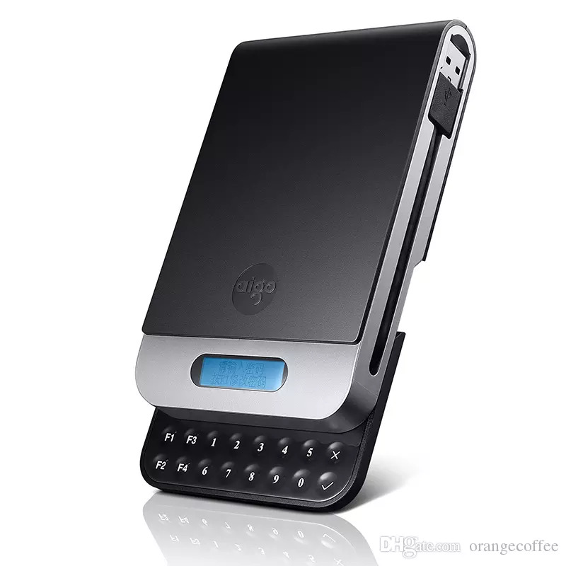
Here I am going to detail how I had fun with one drive a colleague gave me: the Chinese Aigo “Patriot” SK8671, which follows the classical design for external encrypted HDDs: a LCD for information diplay and a keyboard to enter the PIN.
DISCLAIMER: This research was done on my personal time and is not related to my employer.
 |
 |
The user must input a password to access data, which is supposedly encrypted.
Note that the options are very limited:
- the PIN can be changed by pressing
F1before unlocking - the PIN must be between 6 and 9 digits
- there is a wrong PIN counter, which (I think) destroys data when it reaches 15 tries.
In practice, F2, F3 and F4 are useless.
Hardware design
Of course one of the first things we do is tear down everything to identify the various components.
Removing the case is actually boring, with lots of very small screws and plastic to break.
In the end, we get this (note that I soldered the 5 pins header):
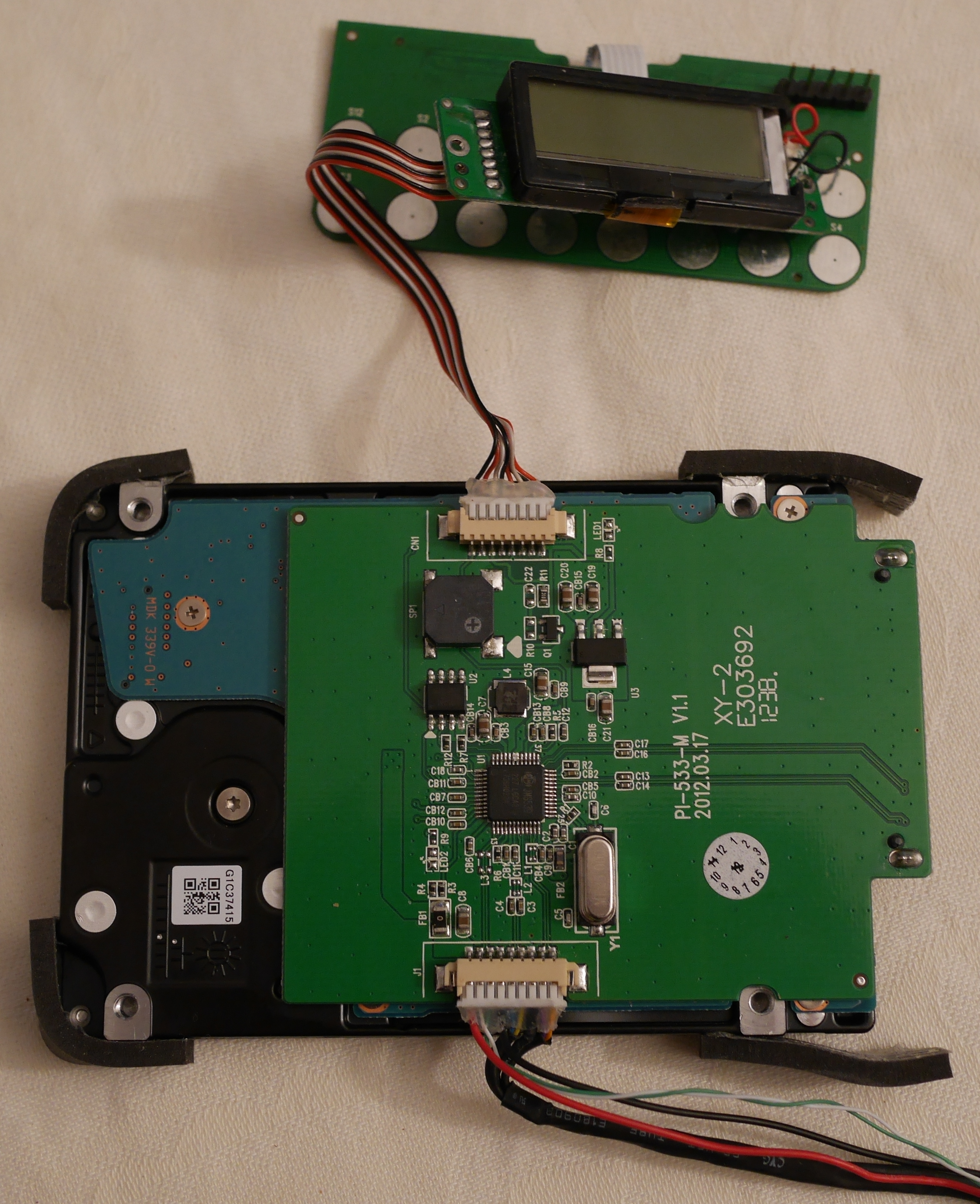
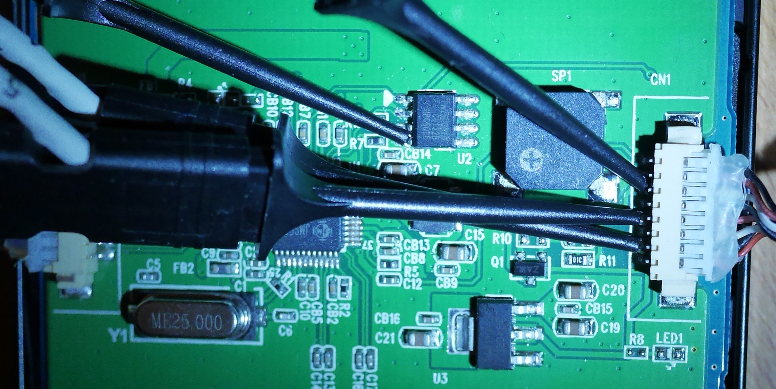
Main PCB
The main PCB is pretty simple:
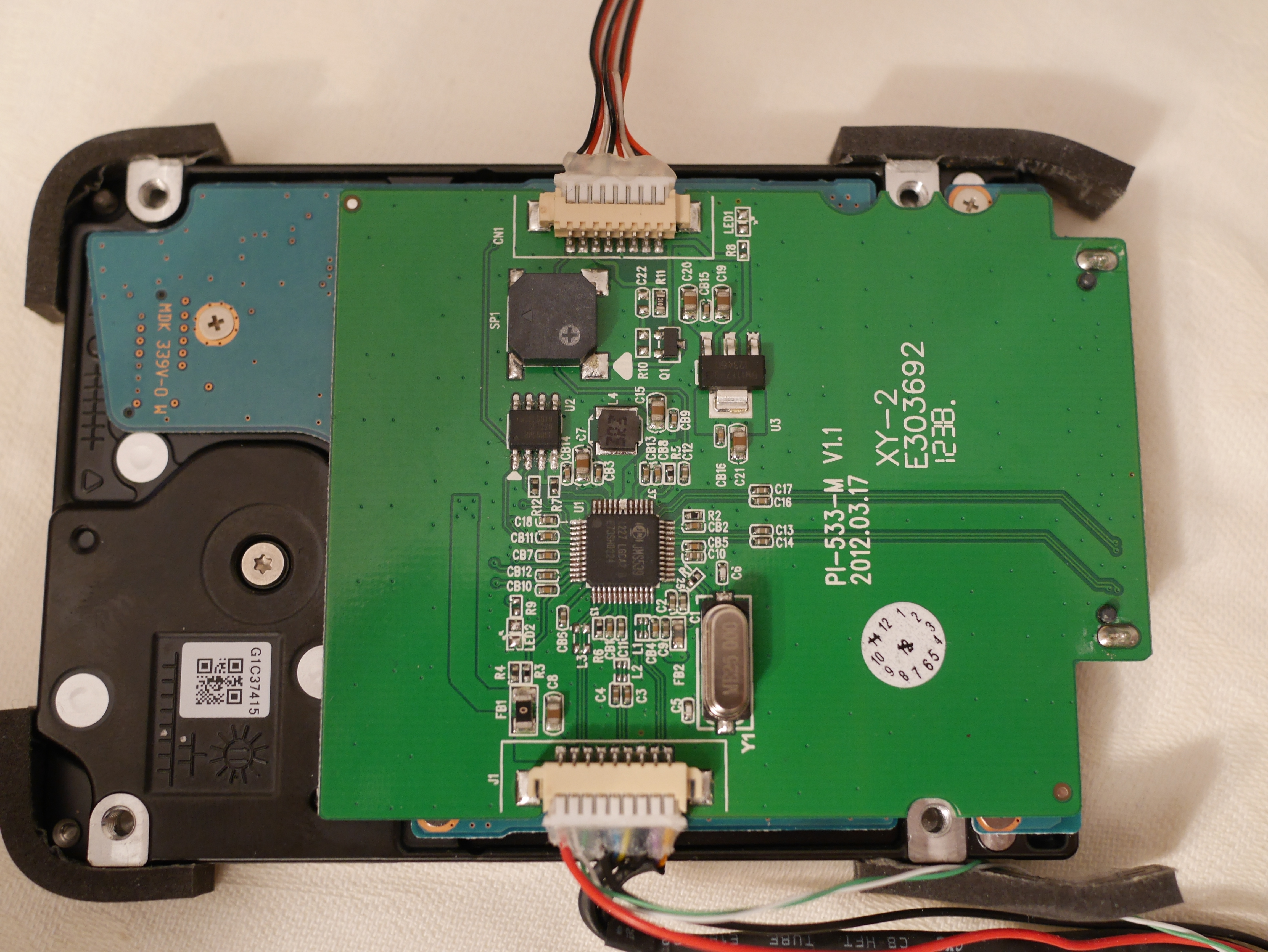
Important parts, from top to bottom:
- connector to the LCD PCB (
CN1) - beeper (
SP1) - Pm25LD010 (datasheet) SPI flash (
U2) - Jmicron JMS539 (datasheet) USB-SATA controller (
U1) - USB 3 connector (
J1)
The SPI flash stores the JMS539 firmware and some settings.
LCD PCB
The LCD PCB is not really interesting:
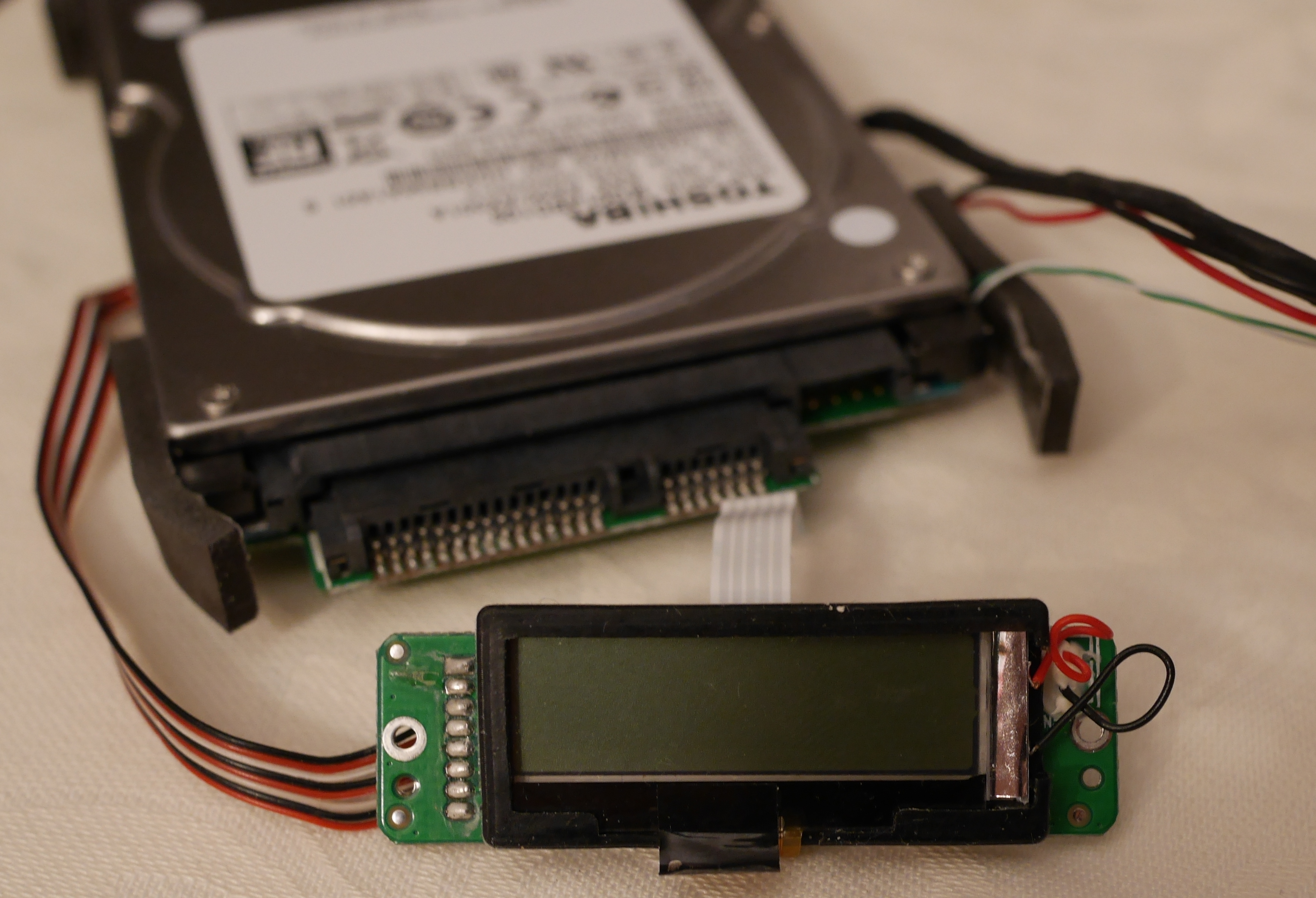
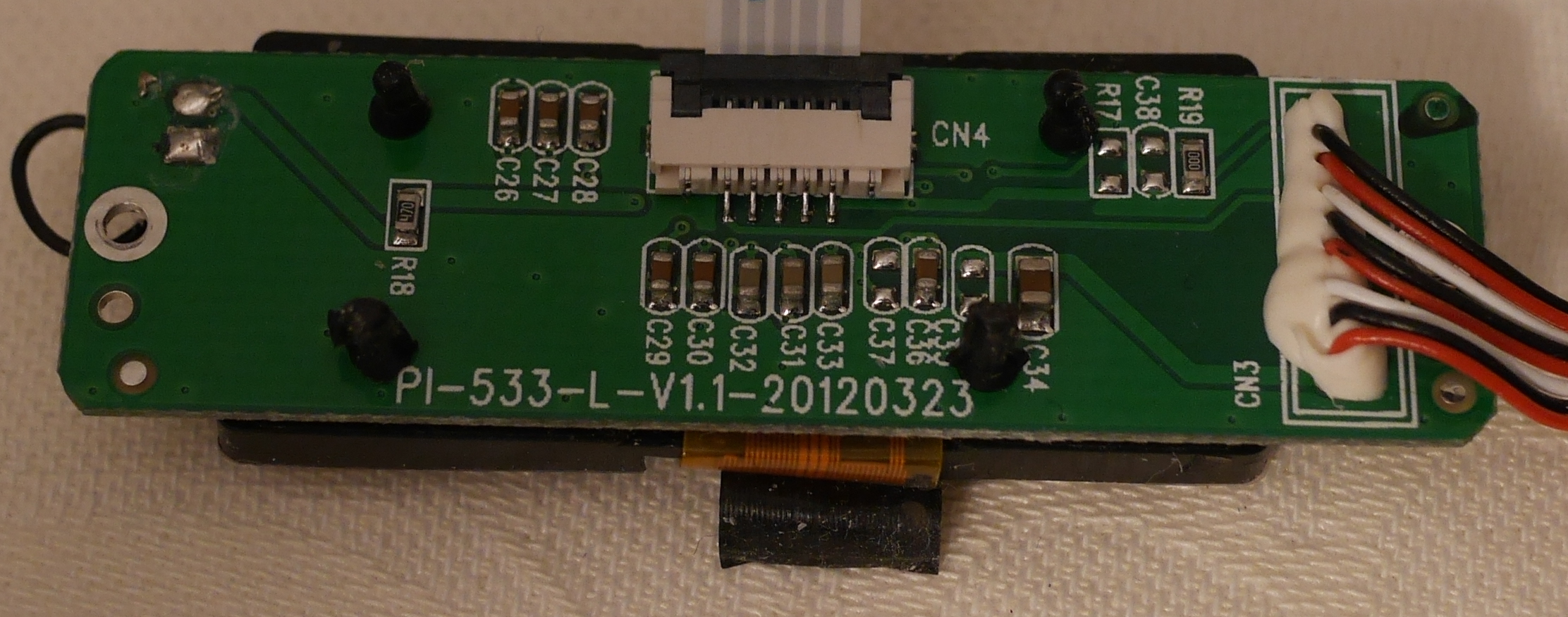
It has:
- an unknown LCD character display (with Chinese fonts probably), with serial control
- a ribbon connector to the keyboard PCB
Keyboard PCB
Things get more interesting when we start to look at the keyboard PCB:
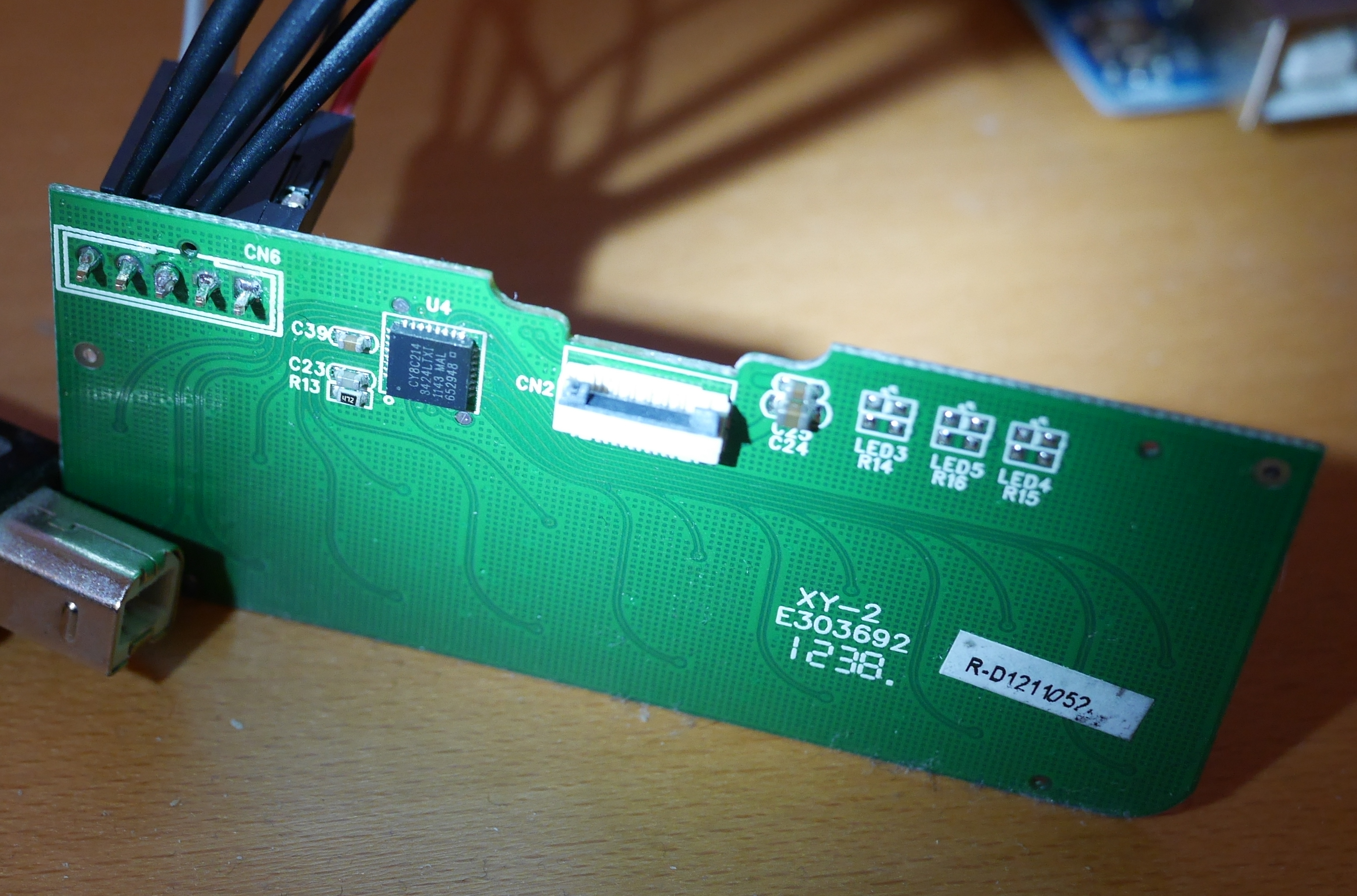
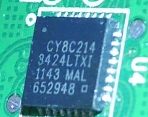
Here, on the back we can see the ribbon connector and a Cypress CY8C21434 PSoC
1 microcontroller (I’ll mostly refer to it as “µC” or “PSoC”):
The CY8C21434 is using the M8C instruction set, which is documented in the
Assembly Language User Guide.
The product page states it supports CapSense, Cypress’ technology for capacitive keyboards, the technology in use here.
You can see the header I soldered, which is the standard ISSP programming header.
Following wires
It is always useful to get an idea of what’s connected to what. Here the PCB has rather big connectors and using a multimeter in continuity testing mode is enough to identify the connections:
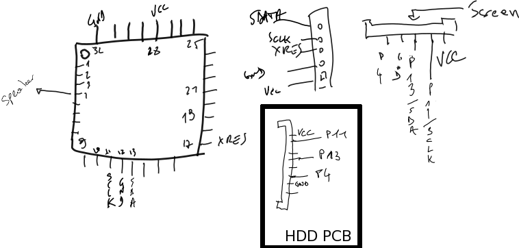
Some help to read this poorly drawn figure:
- the PSoC is represented as in the datasheet
- the next connector on the right is the ISSP header, which thankfully matches what we can find online
- the right most connector is the clip for the ribbon, still on the keyboard PCB
- the black square contains a drawing of the
CN1connector from the main PCB, where the cable goes to the LCD PCB. P11, P13 and P4 are linked to the PSoC pins 11, 13 and 4 through the LCD PCB.
Attack steps
Now that we know what are the different parts, the basic steps would be the same as for the drives analyzed in previous research :
- make sure basic encryption functionnality is there
- find how the encryption keys are generated / stored
- find out where the PIN is verified
However, in practice I was not really focused on breaking the security but more on having fun. So, I did the following steps instead:
- dump the SPI flash content
- try to dump PSoC flash memory (see part 2)
- start writing the blog post
- realize that the communications between the Cypress PSoC and the JMS539 actually contains keyboard presses
- verify that nothing is stored in the SPI when the password is changed
- be too lazy to reverse the 8051 firmware of the JMS539
- TBD: finish analyzing the overall security of the drive (in part 3 ?)
Dumping the SPI flash
Dumping the flash is rather easy:
- connect probes to the
CLK,MOSI,MISOand (optionally)ENpins of the flash - sniff the communications using a logic analyzer (I used a Saleae Logic Pro 16)
- decode the SPI protocol and export the results in CSV
- use decode_spi.rb to parse the results and get a dump
Note that this works very well with the JMS539 as it loads its whole firmware from flash at boot time.
$ decode_spi.rb boot_spi1.csv dump
0.039776 : WRITE DISABLE
0.039777 : JEDEC READ ID
0.039784 : ID 0x7f 0x9d 0x21
---------------------
0.039788 : READ @ 0x0
0x12,0x42,0x00,0xd3,0x22,0x00,
[...]
$ ls --size --block-size=1 dump
49152 dump
$ sha1sum dump
3d9db0dde7b4aadd2b7705a46b5d04e1a1f3b125  dump
Unfortunately it does not seem obviously useful as:
- the content did not change after changing the PIN
- the flash is actually never accessed after boot
So it probably only holds the firmware for the JMicron controller, which embeds a 8051 microcontroller.
Sniffing communications
One way to find which chip is responsible for what is to check communications for interesting timing/content.
As we know, the USB-SATA controller is connected to the screen and the Cypress
µC through the CN1 connector and the two ribbons. So, we hook probes to the 3
relevant pins:
- P4, generic I/O in the datasheet
- P11, I²C SCL in the datasheet
- P13, I²C SDA in the datasheet
We then launch Saleae logic analyzer, set the trigger and enter “123456✓” on the keyboard. Which gives us the following view:
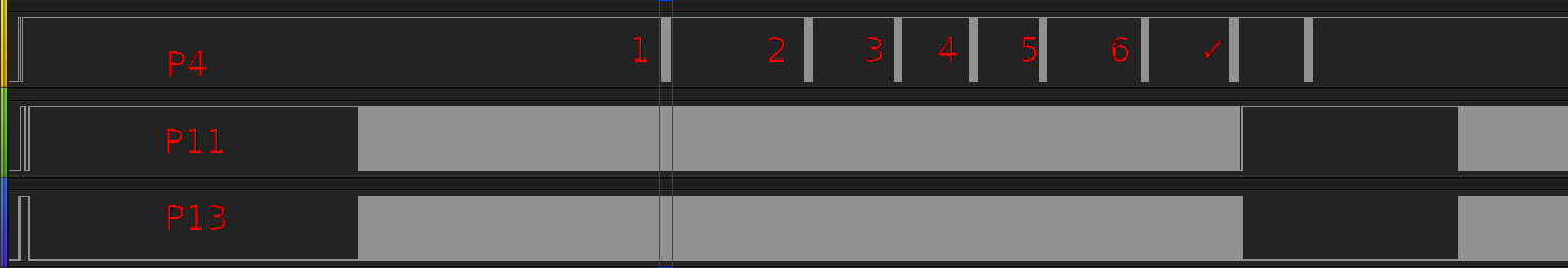
You can see 3 differents types of communications:
- on the P4 channel, some short bursts
- on P11 and P13, almost continuous exchanges
Zooming on the first P4 burst (blue rectangle in previous picture), we get this :
You can see here that P4 is almost 70ms of pure regular signal, which could be a clock. However, after spending some time making sense of this, I realized that it was actually a signal for the “beep” that goes off every time a key is touched… So it is not very useful in itself, however, it is a good marker to know when a keypress was registered by the PSoC.
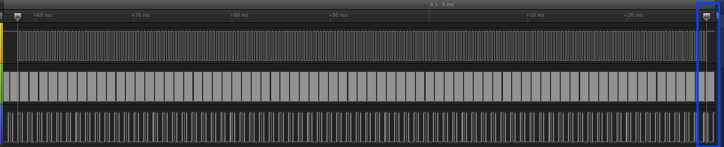
However, we have on extra “beep” in the first picture, which is slightly different: the sound for “wrong pin” !
Going back to our keypresses, when zooming at the end of the beep (see the blue
rectangle again), we get: 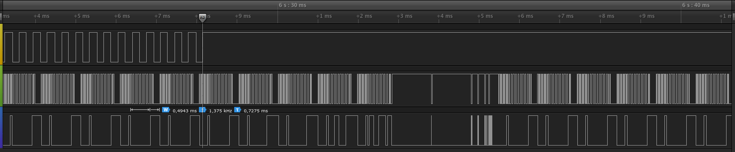
Where we have a regular pattern, with a (probable) clock on P11 and data on P13. Note how the pattern changes after the end of the beep. It could be interesting to see what’s going on here.
2-wires protocols are usually SPI or I²C, and the Cypress datasheet says the
pins correspond to I²C, which is apparently the case:
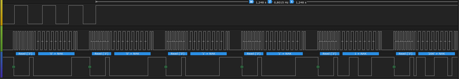
The USB-SATA chipset constantly polls the PSoC to read the key state, which is ‘0’ by default. It then changes to ‘1’ when key ‘1’ was pressed.
The final communication, right after pressing “✓”, is different if a valid PIN is entered. However, for now I have not checked what the actual transmission is and it does not seem that an encryption key is transmitted.
Anyway, see part 2 to read how I did dump the PSoC internal flash.